nand2tetris, Part 1
2022-08-18
"It takes building one yourself to realize you don't deserve a computer."
On 2022-07-22, I finally clicked into the bookmark that had been sitting in my "University readlist" folder, untouched, since last August. Somehow I justed wanted to build a computer all of a sudden.
First a bit of background. Nand to Tetris is a course available online by Noam Nisan and Shimon Shocken that teaches you how to build a modern (albeit extremely simple) computer all the way up from NAND gates. The course is divided in two parts, to which I have given the following nicknames:
- Part 1, NAND to Computer
- Part 2, Computer to Tetris
The first part of the course consists of 6 projects. On 2022-08-16 I completed all of them. In this blogpost I will recap what I learned from the course, and from my mistakes. WARNING: There will be spoilers. If all you need is reasons why you should enroll, go to Course review.
I've uploaded my current projects to this git repo.
Project 01: Elementary gates
In this project I built a few basic logic gates, such as AND, XOR, and the (De)Mux, using a custom HDL language invented for the course. Here is the code for the AND gate:
CHIP And {
    IN a, b;
    OUT out;

    PARTS:
    Nand(a=a, b=b, out=nout);
    Not(in=nout, out=out);
}
Graphically, the HDL describes the following schematic:
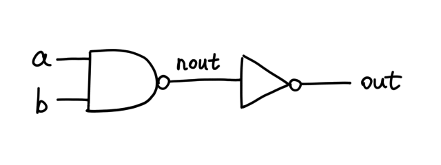
Here a, b and out are hardcoded, but nout is an arbitrary name
I gave to the internal pin. If we further substitute the implementation of
Not in Nand, this is what actually lives on the silicon:
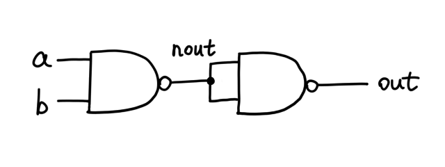
Once we have written this HDL code, we can encapsulate the AND gate in the following symbol, which is in essence two NAND gates in a trenchcoat:
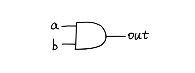
And this is one of the few chips that have so few pins exposed (hence "elementary") that you can craft a truth table for it, and thus can test them manually.
How I built and optimized the XOR gate by toying with boolean expressions (click to expand)
Here is the truth table of XOR, and you have to implement it with chips you already made, which are AND, OR, NOT, and NAND.
 a | b | out
---|---|----
 0 | 0 | 0
 0 | 1 | 1
 1 | 0 | 1
 1 | 1 | 0
The solution is not immediately obvious (you can skip this part if you find it so). It is proven that, given any truth table of finite columns, you can construct a boolean expression satisfying it using what's called a "disjunctive normal form". Here's how it works. First you extract every row that outputs 1:
 a | b | out
---|---|----
 0 | 1 | 1
 1 | 0 | 1
Then we tie a NOT to each 0 input (excuse the pun), thus synthesizing two
sufficient conditions so that out=1:
(NOT a) AND b => out=1
a AND (NOT b) => out=1
Finally, we OR them both, resulting in a single boolean expression:
((NOT a) AND b) OR (a AND (NOT b))
From a pragmatic perspective, our job is done. But the whole premise of nand2tetris is that, we're building every chip out of NAND gates, and I'm challenging myself to use as few as possible. So let's count how many NAND gates we need to make a XOR.
Gate | # of NAND gates
-----|----------------
NAND | 1
NOT  | 1
AND  | 2
OR   | 3
XOR  | ?
((NOT a) AND b) OR (a AND (NOT b))
  ^      ^      ^     ^    ^
  1      2      3     2    1
That's 9 in total. Can we optimize it? Let's try eliminating the OR first,
based on the fact that a OR b = NOT((NOT a) AND (NOT b)):
  ((NOT a) AND b) OR (a AND (NOT b))
= NOT((NOT((NOT a) AND b)) AND (NOT(a AND (NOTb))))
At first glance this might seem more complicated, but remember,
NOT(a AND b) = a NAND b… which is exactly our atomic building
block! We continue our equation:
= ((NOT a) NAND b) NAND (a NAND (NOT b))
Since NOT and NAND are both made of one single gate, our optimized number of gates is 5. (However, this optimization did not matter for a reason I will explain later.)
There were many other chips I was already familiar with, so I implemented them with little trouble apart from the HDL syntax.
Project 02: ALU
The goal of building a computer in this theoretical approach is to conjure up a way to make a pool of NAND gates capable of thinking. This project does exactly that. Yes, you are right: I built an ALU.
The fundamental idea of an ALU is that, you give it two inputs x and y
and pick a function h, and for some reason it outputs h(x, y) where
h is one of the following:
0, 1, -1,                // constant value
x+y, x-y, y-x            // arithmetics
x, y, -x, -y, !x, !y,    // single variable function
x+1, y+1, x-1, y-1,        // one variable + constant
x&y, x|y                // boolean operation
You supply 6 bits known as "control bits" that let the ALU decide what function you want. They are:
zx,zy: coerce x or y to zero when setnx,ny: negate x or y when set (binary NOT)f: performs binary arithmetics when set, boolean operation otherwiseno: negate output-to-be
But how do you know when you need to negate or zero the operands? Doesn't
this call for an if statement? Well, in project 01 I made a chip named
Mux16 and it is tremendously helpful. It's the hardware embodiment of
if () ... else ....
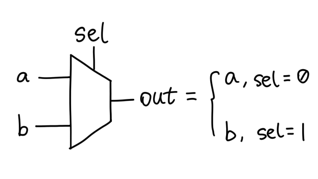
(In reality we are using the 16-bit version, but in principle they're the same.)
This means I just need to hook nx and zx to sel pins, and route
a's and b's somewhere.
The HDL that does this job for x is:
Mux16(a=x, b=false, sel=zx, out=zdx);    // false = all 0's
Not16(in=zdx, out=ndx);
Mux16(a=zdx, b=ndx, sel=nx, out=px);
Graphically:
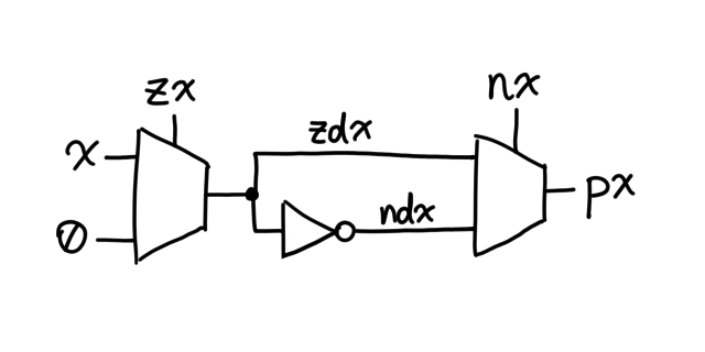
(The order of the muxes matters, because when zx = nx = 1, this logic
configuration yields ~0 = -1 while the other way gives you 0.)
The same goes for y. Now that we have the processed version of x and
y, denoted px and py, it's time to force this pile of imaginary NAND
gates to do math for us. The boolean AND operation is trivial, so we will
only be talking about the Adder, which is a chip that takes two binary
numbers x and y and outputs (x+y) % 65536, that is, carries every
bit except the MSB.
But wait! Didn't we just see "x-y" and "y-x"? How can an Adder possibly do
that? Note that there is no "Subtractor"; to do x-y you simply calculate
~(~x + y) where ~ denotes bitwise negation, thanks to 2's complement.
Proof that x-y = ~(~x + y)
We know in 2's complement,
~x + x = 0xffff = -1 <==> ~x = -1 - x
Add y to both sides, we get
~x + y = -1 - x + y
Therefore, by means of negation,
~(~x + y) = -1 - (~x + y)
          = -1 - (-1 - x + y)
          = -1 + 1 + x - y
          = x - y             ⌷
(Nisan and Shocken have supplied this course with a table where you can look up the ALU output given six control bits, or vice versa, but it won't be a necessity until project 06.)
In addition to a 16-bit output bus (we call a group of indexable pins
a "bus"), the ALU outputs two flags: ng and zr. If the final output is
negative, ng is set; if it is zero, zr is set. The clever thing is,
ng is just the highest bit of the output, i.e. out[15], and zr is
set iff every bit in out is zero.
That's it, we have completed the ALU! I know y'all are anticipating the schematics; how can I let you down?
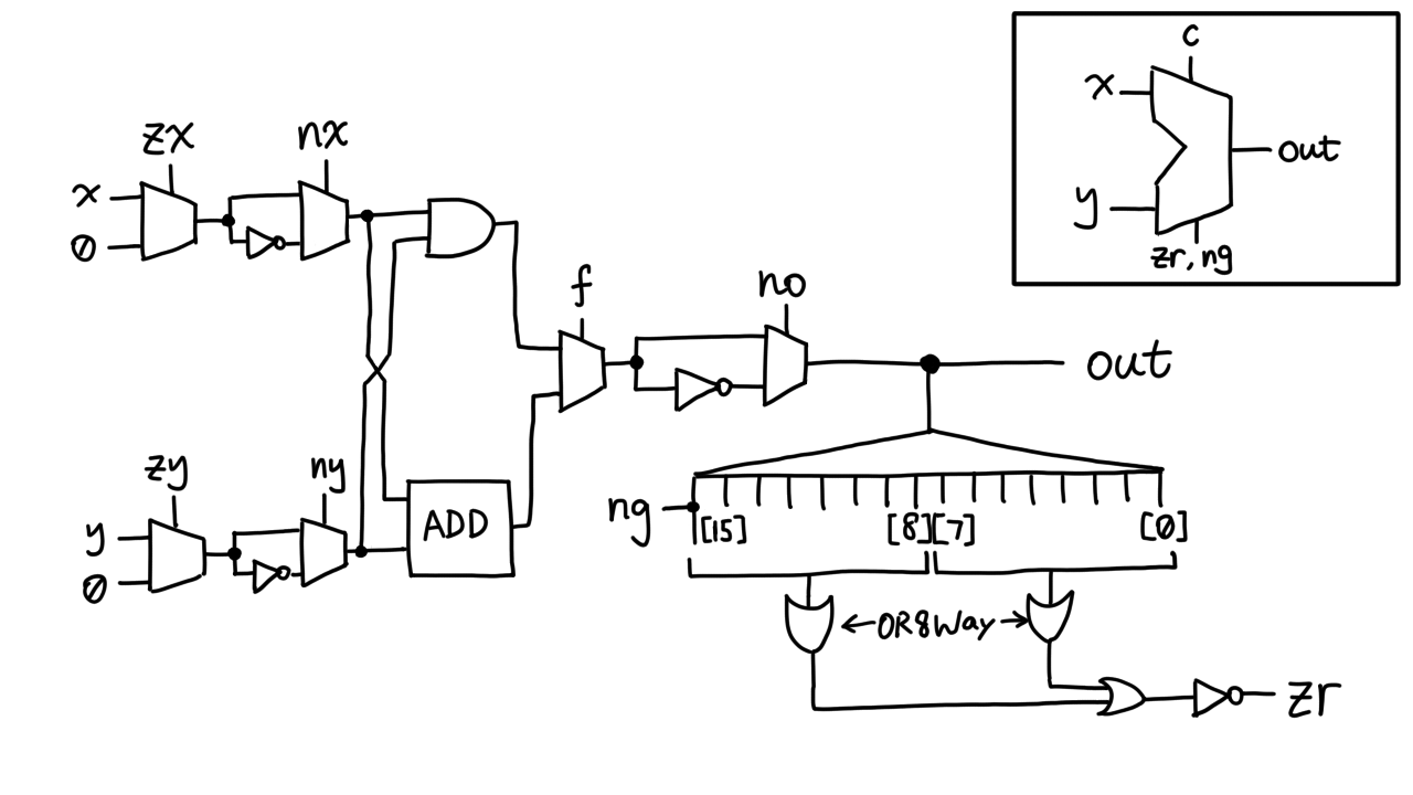
For some reason nand2tetris only provided me with Or8Way, which OR's
together 8 bits, so I had to use two of them to do all 16. I tried writing
an Or16Way "helper chip" in the project 01 folder, but when I tried to
include it in the ALU, it did not work. Why?
When you tell the hardware simulator to load a chip, it first looks for
<chip_name>.hdl under the working directory; if there's no such file, it
proceeds to look for builtin chips implemented in Java. No other directory
is in its path, even project 01. This explains why the optimization I made
in project 01 does not matter.
If it did matter, how many NANDs are there in this ALU?
It's Python scripting time! I just need to recursively find out how many NANDs in each subchip, then add them up. The syntax of HDL is pretty simple, and the script goes as follows (simplified):
HDL_PROJECTS = ["01", "02", "03/a", "03/b", "05"]

CHIPS = {
    "Nand": 1,
    "DFF": 6,  # https://commons.wikimedia.org/wiki/File:Edge_triggered_D_flip_flop.svg
}


def count_nands(project_path, chip):
    # figure out where the HDL is
    f = None
    for dir in HDL_PROJECTS:
        try:
            f = open(project_path + dir + f"/{chip}.hdl")
            break
        except FileNotFoundError:
            continue

    if f is None:
        print(f"Chip not found: {chip}", file=stderr)
        return 0

    while f.readline().strip() != "PARTS:":
        continue

    nands = 0
    line = f.readline()  # e.g. "    Not (in=in, out=out); // comment"
    while line:
        code = line.split("//")[0].strip()  # e.g. "Not (in=in, out=out);"
        if "(" not in code:
            line = f.readline()
            continue
        subchip = code.split("(")[0].strip()  # e.g. "Not"
        if subchip not in CHIPS:
            CHIPS[subchip] = count_nands(project_path, subchip)
            print(f"{subchip}\t{CHIPS[subchip]}")

        nands += CHIPS[subchip]
        line = f.readline()

    f.close()
    return nands

chip = "ALU"
nands = count_nands("/path/to/nand2tetris/projects/", chip)
print(f"There are {nands} NAND gates in {chip}")
The output is (vertically aligned):
Not             1
And             2
Or              3
Mux             8
Mux16           128
Not16           16
And16           32
Xor             5
HalfAdder       7
FullAdder       17
Add16           262
Or8Way          21
There are 1156 NAND gates in ALU
Pretty sure my algorithm's right. Honestly it's fewer gates than I imagined because the ALU seemed to do so many things.
Most of the chips I made in project 02 are too complex to test by hand, but fortunately nand2tetris provides test scripts and compare files you can run in a hardware simulator that simulates the logic described by the HDL.
While I was drawing the schematics, a question came to mind: If I set f
to zero, will the Adder be working the same way as if f=1?
Answer
Yes, it will. Simply put, chips "downstream" do not directly affect those "upstream" as far as this course is concerned. The implication is that, when you give an x and a y to the ALU, it does both computations at once: boolean AND and binary addition. It is the Mux's job to select which branch to pass downstream, and which one to discard. This is, in a stretch, called speculative execution
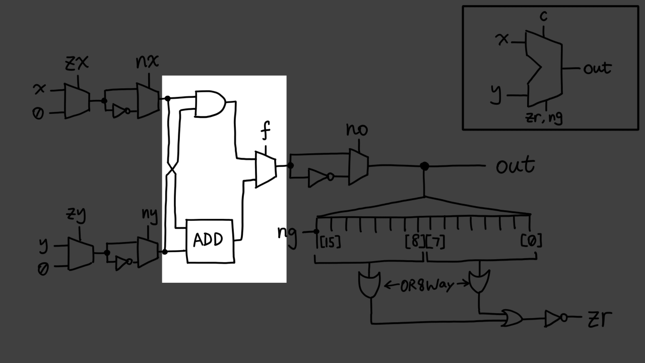
As you see in the highlighted area, both of these gates are
switching internally, and both of them consume power, even when one of
them does not generate useful output. Recall the if statement
in programming:
if (boolean) {
    do_a();
} else {
    do_b();
}
Either but not both of do_a or do_b will be run.
This is one of the major mindblowers I came into, and I think it's worth
writing about it.
Project 03: Memory
In project 02 we made an ALU think, but only once. This is because it doesn't remember anything. So if we want to build a computer, we need to make something that keep a record of what has been done, and what is left to do.
The D flip-flop (DFF) is a chip that remembers one bit of information for
one clock cycle. It's the fundamental building block for sequential logic
in nand2tetris. Limitations in the simulator forbid building it from NAND
gates yourself, because to do that you would need to wire an output into
the input, which forms an infinite loop which the simulator is incapable
of resolving. Instead, it provides a builtin chip, DFF, using which you
can build registers from 1 bit to 16K words.
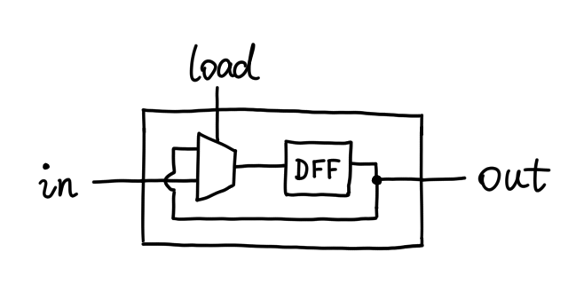
Here's how a register works from the user's point of view:
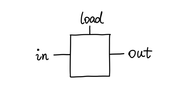
If you give it some data via in and pull load to logic one, the data
will show up in out at the next clock cycle. However as long as load
remains zero, out does not change, as if "remembering" the data.
But doesn't the D flip-flop only keep its data for one clock cycle? Yes,
but we can find our way around it. We simply use a Mux as a "valve": it
only lets in pass through when load is high. Otherwise, we feed out
into the DFF again, creating an eternal feedback loop, but this time the
simulator handles it with no problem, because the loop is delayed by one
clock cycle each step.
The RAM I proceeded to build is just an array of arrays of arrays of … of arrays of registers. Just copy and paste; no thinking required.
The Program Counter (PC for short) however, ground my brains like jelly in
a blender. Its job is to remember a number, increment it by one each clock
cycle, and set it to some other value when required. The user controls it
using three control pins: load, inc, and reset. The increment
happens when inc=1, unless load=1, in which case the PC swallows the
data on the in bus and spits it out at the next clock cycle, then
increment that value from now on. reset, of course, forces the output to
zero.
It's not hard to think of using the Register for storage and Inc16 (16-bit incrementer) to do the math. The rest is Muxes, just like this:
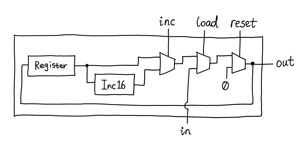
There is a problem with this solution. Do you see it? Let's read the chip specs again carefully:
if      (reset[t] == 1) out[t+1] = 0
else if (load[t] == 1)  out[t+1] = in[t]
else if (inc[t] == 1)   out[t+1] = out[t] + 1  (integer addition)
else                    out[t+1] = out[t]
Note that the first line tells us that out should be zero if reset at
the previous clock cycle is one, whereas in the schematic above, out
becomes zero as soon as reset rises to one, because the Mux is
a combinatorial chip — it does not wait for the clock. So what can we do?
We just need a way to delay out by one clock cycle. The only sequential
chip here is the Register, so let's try hooking out onto its output
instead:
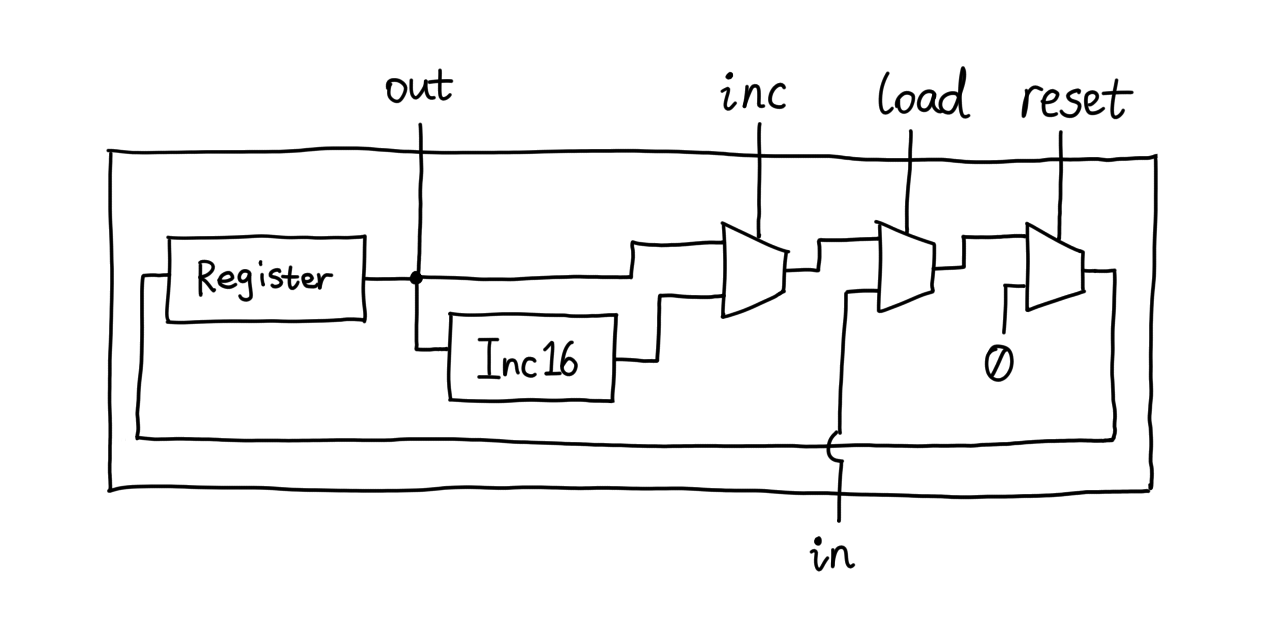
Simulation tells me that this works perfectly, but deep inside I feel I'm still extremely sloppy at clocked logic.
Project 04: Assembly
There's no HDL in project 04. Instead, I learned to write assembly. Nisan and Shocken, once again, invented an assembly language for this very architecture called HACK. The language understands two sorts of instructions. But first, we need to imagine we have a computer.
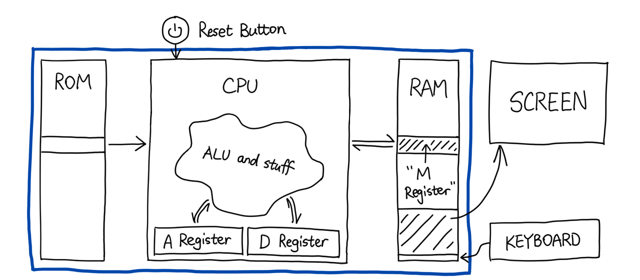
Here you see three devices inside the blue rectangle: ROM, CPU, and RAM.
- ROM: Read-Only Memory. Our computer fetches and executes instructions from it. We did not write HDL for it because it's just a read-only version of the RAM, and it's builtin.
- CPU: An encapsulation of the ALU that works by black magic until project 05.
- RAM: Random Access Memory. Our computer can read and write data in it.
HACK assembly provides an extremely rudimentary way to control the CPU. The key to understanding HACK assembly is the three registers: D, A, and M. D stands for "Data" (probably). It holds a 16-bit value; so do the other two. You can do two things to it in our assembly language:
- Read it as an ALU input
- Write ALU result into it
A stands for "Address". It works pretty much the same way D does, with one more added function:
- Set it to an assemble-time constant
which can be realized using this line of assembly (or instruction):
@42
Expand to learn more about the difference between A and D
In HACK assembly, the A register is the only one you can directly assign an value to, like we just did. In contrast, if you want to write 42 into D, you will need to go through two steps:
@42     // this sets A to 42
D=A     // this copies the value of A, 42, into D
However, if you need to set A to some non-constant, you have to use another trick:
A=D // this sets A to current value of D
M stands for "Memory". Note that it is not a register in the literal sense; it is actually an alias for RAM[A]. For example,
@42
M=-1
sets the 42nd word (if you count from zero) in RAM to -1, i.e. set all bits to one.
We call an instruction an "A-instruction" if it begins with "@" and "C-instruction" otherwise. By executing a C-instruction the ALU always computes something — even zero. You can prefix it with a destination to decide where the result should be saved. You can either pick or not pick any of the three registers, A, D, and M, resulting in 8 possibilities, like this:
D+M;    // compute D+M, but do not save it anywhere
AD=1;   // set A and D to 1 simultaneously
AMD=1   // set A, M and D to 1 simultaneously
C-instructions can also do something really cool, which is jumping. The syntax is different from what you might find in an industrial assembly language.
@42
D;JEQ   // this jumps to ROM[42] if D=0
The JEQ here is a jump instruction. A jump instruction
compares ALU output to zero, and jumps if it is greater/equal/not
equal/etc.
What if I want to jump to 42 if RAM[69] is zero?
Can I just:
@69
@42
M;JEQ   // does this work?
No. @42 completely overwrote @69, so the M on
line 3 is actually RAM[42]. To perform this maneuver, we need to make use
of D.
@69     // set A to 69
D=M     // D is now RAM[69]
@42     // set A to 42
D;JEQ   // if D=0, jump to ROM[42]
For convenience, we can attach a label to an instruction in assembly and reuse it later:
(END)
@END
0;JMP
In this code (END) points to @END, and JMP is an unconditional jump,
so this creates an infinite loop. It is good practice to terminate
a program with this, lest the ROM address overflows and the computer runs
the program again from instruction 0.
You can also use custom symbols after an "@" to assign or reuse a static address starting from 16. It is like declaring a variable whose value is stored in RAM[n] where n ≥ 16. Why not 0-15, you ask? Well, they are reserved for symbols R0-R15.
This @symbol notation goes further by mapping a monochrome screen to
a memory area @SCREEN, namely 16384-24575, and a keyboard to @KBD,
which is 24576. If you write the highest bit to one in RAM[16384], you
paint the top left pixel black. If you press space, it sets RAM[24576] to
32 (0x20). You can interact with them in the CPU emulator.
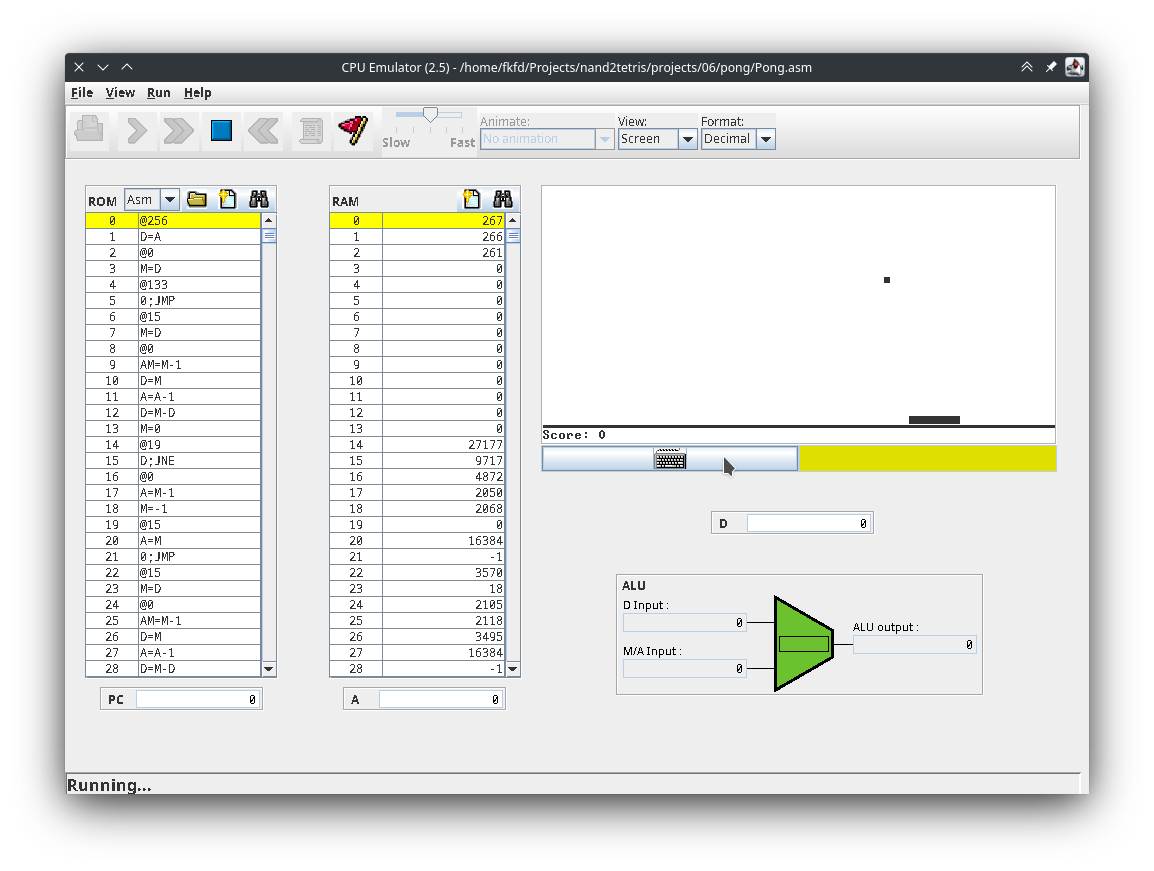
▲ CPU Emulator running Pong
Here's a snippet of HACK assembly I wrote that increments RAM[16] from 0 until it is equal to whatever you put in RAM[0] before running the program:
@x
M=0     // x = RAM[16] = 0

(LOOP)
@R0
D=M     // D = RAM[0]
@x
D=D-M   // D -= x
@END
D;JEQ   // if D == 0 goto END
@x
M=M+1   // otherwise x += 1
@LOOP
0;JMP   // goto LOOP

(END)
@END
0;JMP
Project 05: Computer
After a project that seemed to come out of nowhere, it sounds reassuring that we're back to building the computer hardware. First we need to decide the architecture. It is common to build a computer on the Von Neumann architecture. But canon Von Neumann stores both instructions and data in a single memory unit, commonly RAM, so the CPU can modify both. But even so, a tiny ROM is needed to instruct the CPU in its booting process. In our application however, we will just straightforward use two units simiar in size. This means given a single ROM, our computer can only run one specific program. This is called the Harvard architecture, technically a subset of Von Neumann. AVR microcontrollers also use this architecture.
So this means there will be three things inside the computer: CPU, ROM, and RAM. Since we made RAM in project 03 and ROM is builtin, all that's left is the CPU.
The CPU needs to:
- Read instruction from ROM
- Read data from RAM
- Compute something
- Write data to A, D, and RAM
- Run instruction one by one
- Jump to another instruction if programmer asks it to
The instant I read the requirements, I knew there will be a ton of internal wires. Fortunately, the authors provided a block diagram similar to this one:
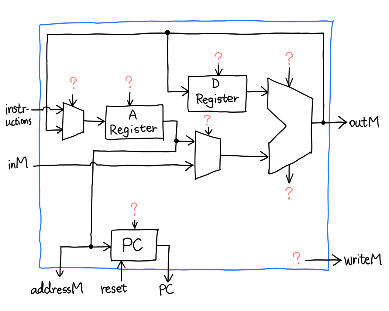
Yikes! What's with the question marks? Apparently it's the authors' own version of spoiler alerts. I had to figure out what they are by myself, and that's a good thing. I like challenges.
Let's first make sure we know what each pin/chip is doing.
- Instruction in ROM comes from pin
instruction - Data from RAM come from pin
inM - Both RAM and ROM addresses are selected using
addressM - The ALU takes two registers and churns out an output
- The A and D Register accept inputs from ALU
- ALU output also goes to RAM via
outM writeMtells RAM to load data- The PC increments, resets or jumps to instruction
What's an instruction anyway? It's a 16-bit value that describes what we want the CPU to do in this clock cycle. An assembler, which we will write in project 06, translates assembly to binary code, but in this project let's assume it came from nowhere.
What the 16 bits represent depends on the type of instruction you're writing. It is specified by the highest bit, called the opcode. In an A-instruction, the opcode is 0, which is followed by 15 bits of address. Considering the size of our larger memory unit, ROM, is 32768 words, 15 makes sense. In this case the CPU will store the value in the A register.
The C-instruction with opcode 1 is more complicated, but boils down to four groups of control bits:
 fixed    ALU control    jump instruction
\     /   \        /        \        /
+-----+---+--------+--------+--------+
| 111 | a | c1..c6 | d1..d3 | j1..j3 |
+-----+---+--------+--------+--------+
      /   \        /        \
       A/M         destination
adecides whether the ALU takes in D and A, or D and M.c1..c6correspond to control bits on the ALU.d1..d3tell CPU to save ALU output to A, D, and M respectively.j1..j3tell CPU to jump to ROM[A] when ALU output <0, =0, and >0, respectively.
In a hunch, it seems we have the answer to most of the question marks.
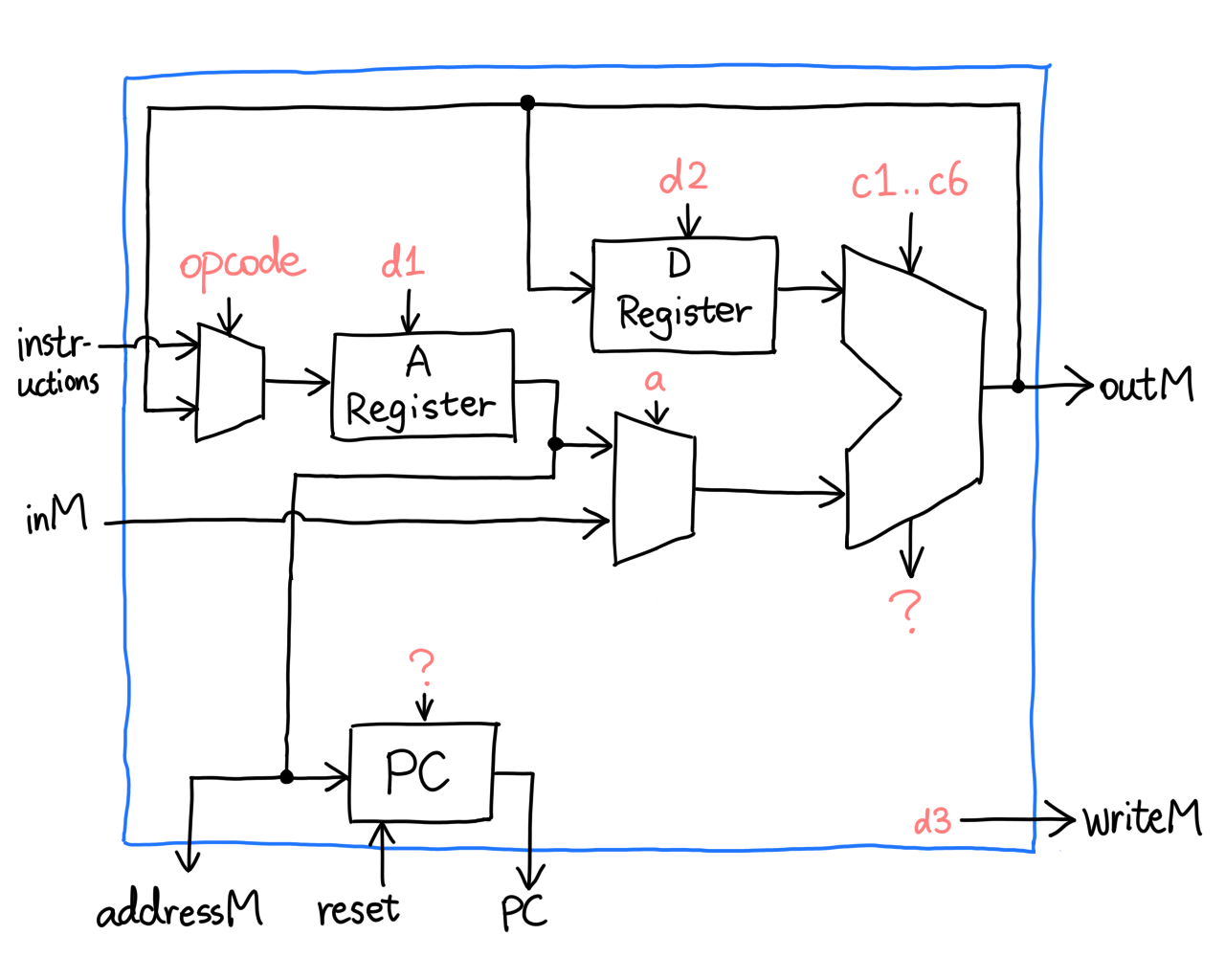
This is simple but wrong. Let's take a close look at the load pin
labeled d1 on the A register. If we try to load address 1 into it, using
an A-instruction @1, what will happen? Let's assemble it:
0000 0000 0000 0001
^\________________/
|        ^
|        |
opcode   integer value 1
The mux on the left will let the instruction through because opcode is
0, but remember, HDL doesn't recognize d1, it only recognizes
instruction[5]. What's gonna happen is, the A register will refuse to
load, because instruction[5] is zero. Something similar will also happen
to d2 and d3, so we add a little logic:
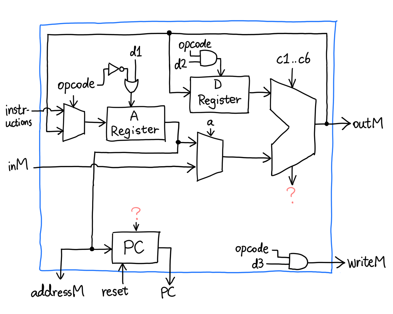
This ensures that A, D and M load data if and only if we explicitly tell
them to. Now we shift our attention to the only two question marks left:
zr and ng coming from the ALU, and load going into the PC.
Notice something? j1..j3 are missing, so it's definitely them. Recall
that we can set the PC to its input if we pull load to high, and this
way we can jump to ROM[A]. But how?
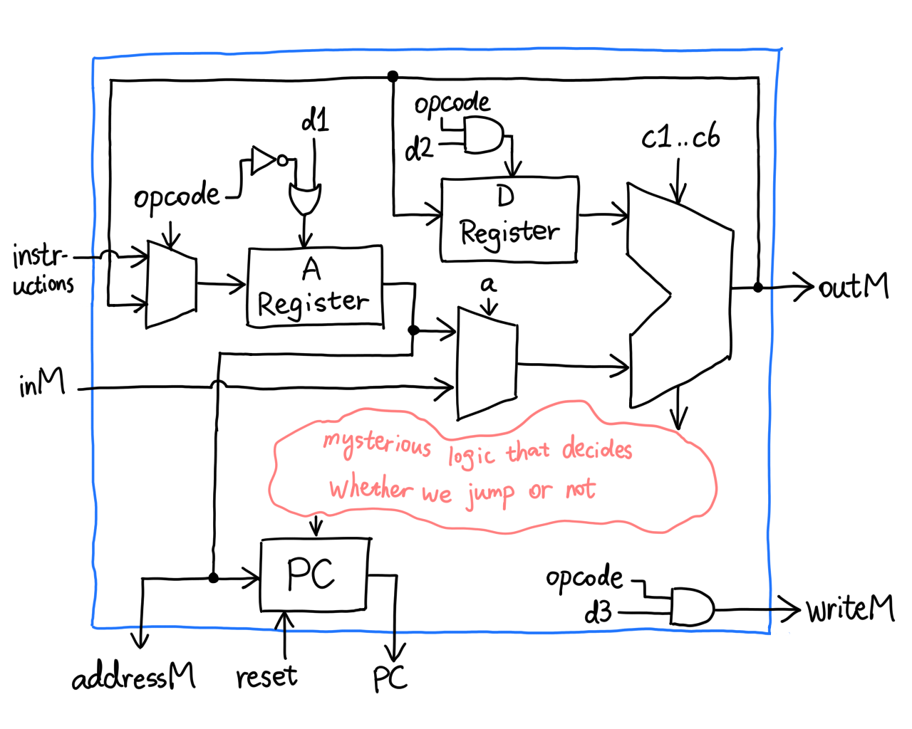
It's actually very straightforward! Apparently the authors thought it through when specifying the ALU.
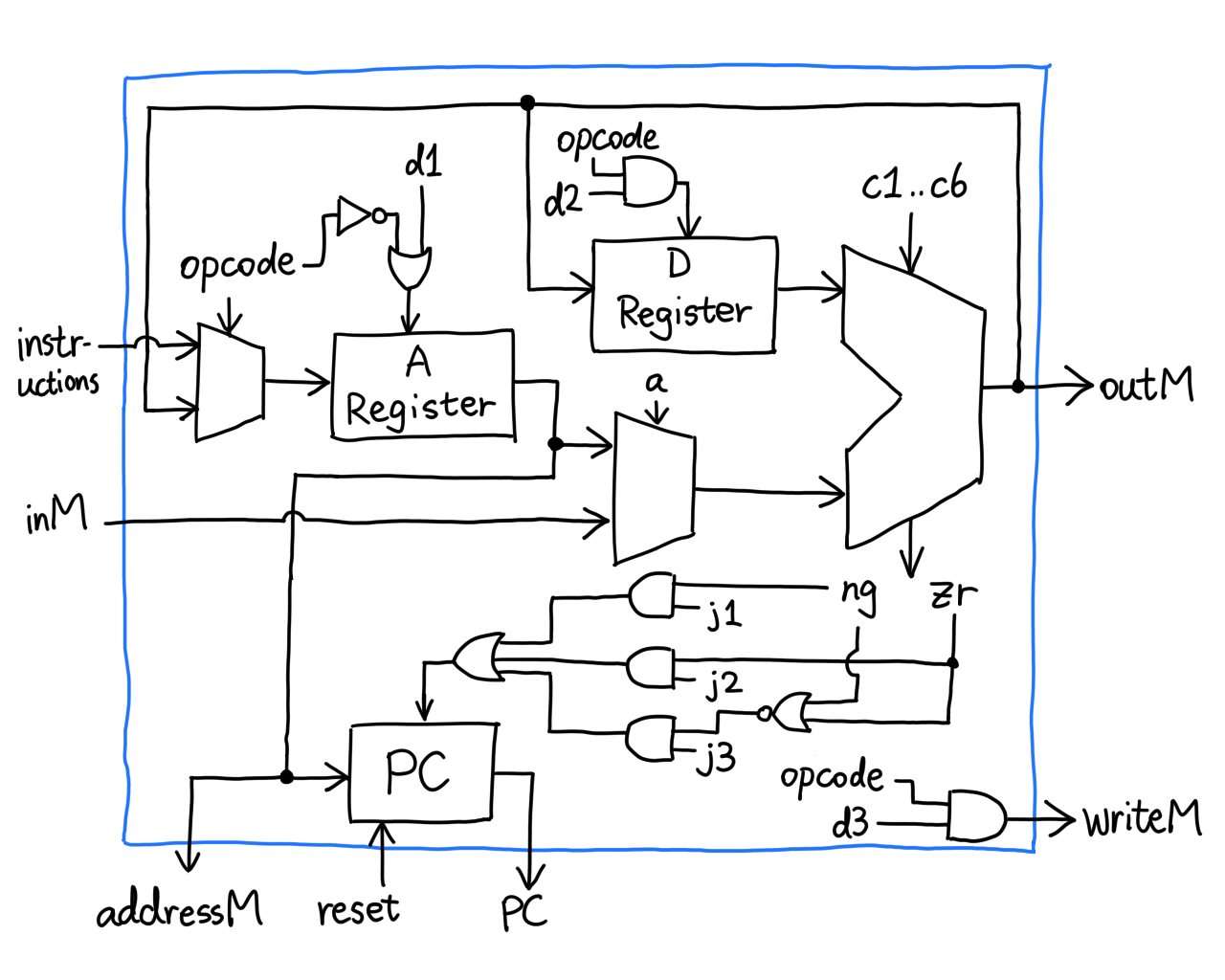
(Actual gates may differ)
And that's it, we made a CPU! We are super close to the computer; all we need to do is connect all the wires. I'm feeling too tired to sketch up another diagram so here's the HDL:
CHIP Computer {
    IN reset;

    PARTS:
    ROM32K(address=pc, out=instruction);
    CPU(
        inM=inM, instruction=instruction, reset=reset,
        writeM=writeM, outM=outM, addressM=addressM, pc=pc
    );
    Memory(in=outM, address=addressM, load=writeM, out=inM);
}
Project 06: Assembler
Having gone through project 04 and 05, if you think something's missing, then you're right. We haven't talked about how we translate assembly to binary instructions. In nand2tetris, you are asked to write an assembler in any high-level language (or not write one at all and assemble by hand). As the grammar is pretty simple and well-defined, it wouldn't take too much effort, yes?
For some reason my self-obsessive ass, after two successful projects in C (one of them being SIRTET), decided to write the assembler in this very cursed language.
Roast me all you want, but most of the time I'm thinking about stuff like "what if the programmer slid in illegal characters in the variable name" and "hmm so I malloc a piece of memory and strcpy the second to second-to-last characters from this string. We'll need a null terminator so the size has to be one byte smaller than the source string blah blah blah" and I'll take another minute to decide how long this piece of memory will live until I free it.
I shall skip the part where I wrote the program because that will bore you
and me to death. Instead, let's watch the results if we assemble the
assembly I showed you in project 04. The
executable is called hack-as, just like avr-as.
$ ./hack-as -v test/inc.asm
====== SYMBOLS =====
label   addr
LOOP    2
END     12
x       16

====== RESULTS =====
addr    binary                  inst
0       0000000000010000        @16
1       1110101010001000        M=0
2       0000000000000000        @0
3       1111110000010000        D=M
4       0000000000010000        @16
5       1111010011010000        D=D-M
6       0000000000001100        @12
7       1110001100000010        D;JEQ
8       0000000000010000        @16
9       1111110111001000        M=M+1
10      0000000000000010        @2
11      1110101010000111        0;JMP
12      0000000000001100        @12
13      1110101010000111        0;JMP

Binary written to test/inc.hack

$ cat test/inc.hack
0000000000010000
1110101010001000
0000000000000000
1111110000010000
0000000000010000
1111010011010000
0000000000001100
1110001100000010
0000000000010000
1111110111001000
0000000000000010
1110101010000111
0000000000001100
1110101010000111
nand2tetris provided me with a few other assembly files I can test my assembler against. The longest one was over 28k instructions. All of them passed.
As always, I did some memory profiling with valgrind:
$ valgrind --leak-check=full --show-leak-kinds=all ./hack-as test/inc.asm
==31030== Memcheck, a memory error detector
...
Binary written to test/inc.hack
==31030==
==31030== HEAP SUMMARY:
==31030==     in use at exit: 0 bytes in 0 blocks
==31030==   total heap usage: 49 allocs, 49 frees, 77,587 bytes allocated
==31030==
==31030== All heap blocks were freed -- no leaks are possible
==31030==
==31030== For lists of detected and suppressed errors, rerun with: -s
==31030== ERROR SUMMARY: 0 errors from 0 contexts (suppressed: 0 from 0)
(It is indeed weird that it needs 77kB of heap memory, but since we've been overdoing it all along we might as well just ignore it.)
The whole process took one night, one day, and one morning. And the afternoon following that morning, I decided to implement it again using Python to see how much easier it is.
The advantage of Python over C is human-oriented string methods like
str.split and str.partition. Also, no manual memory management.
I finished it in less than an hour, not because Python is easy, but
because I already have C code to refer to. This, in hindsight, is a big
mistake. I should have prototyped it in Python first, then proceed to
write it in C. However the speed benefit C provides is an overkill for
this kind of simple task, so in that case I might just not write C at all.
And thus we have bridged the gap between assembly language and machine code. Our computer can run anything. (As long as it fits in the ROM)
Course review
Conceptual
nand2tetris part 1 takes you on a journey from NAND gates as promised. You climb a ladder from the humble logic gate to more and more complex chips, representing increasingly advanced logic, but they're NANDs all the way down. The authors say that the goal of nand2tetris is to "demystify computers": Every time you witness the very chip you made do something exciting, like adding up two numbers or remembering 16 bits of data, one layer of mystery dissolves, because you know X happens when chip Y does Z, not because TSMC soaked your wafer in .25 mol/L holy water. Philosophical takeaway: One complicated thing is just many simple things arranged in a clever way.
Technical
The project-oriented approach really gets your hands dirty, but not completely covered in copper particles thanks to its simulators. They are offered in a software suite, which verifies your work against test scripts bundled along. This is the best thing of this course. If you grab some university textbook, the first chapter might be like "OK now go download NI® Multisim™ for 628 dollars" or "we'll give you an answer to every question and you just need to convince yourself it works", whereas the nand2tetris software suite is GPL'd. I only have two points of criticism:
- It is buggy at times (the safe kind, you just need to restart it)
- It is written in Java (I have a prejudice against everything Java)
As I mentioned in Project 02, every time you advance into a new project, all the chips you've made thus far become builtin Java code instead of HDL. For example, when you simulate the ALU, the Mux/And16/whatever you're seeing is no longer what you wrote in project 01, but part of the simulator itself.
Pro: Complex chips run more efficiently and reliably.
Con: You can't verify your prior chips actually works beyond the test scripts.
Of course, the pro beats the con by an order of magnitude. Don't you have this deep-rooted fear that one loose jumper wire on the breadboard can knock your Ben Eater-style computer completely off the rail?
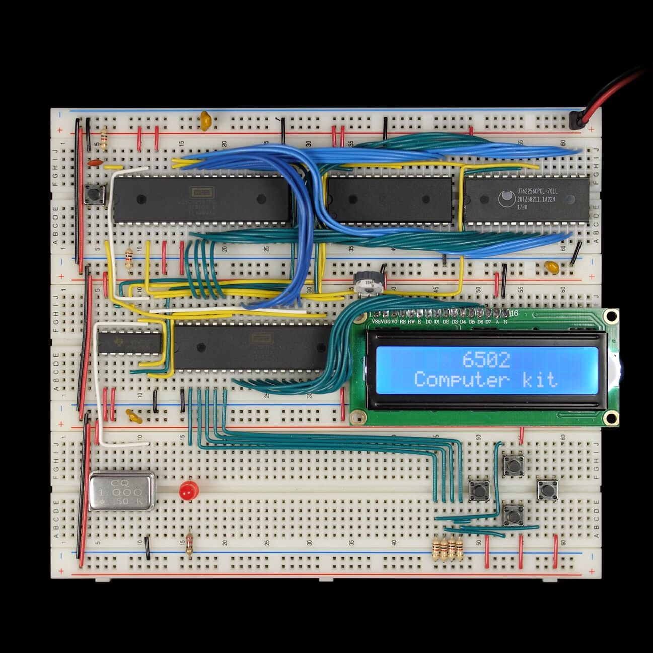
▲ Image credit: Ben Eater, "Build a 6502 computer"
Course outcome
The purpose of this course is, in my opinion, to prove to you that computers are not magic, and that it is possible to build your own computer. It's like one of those workshops that lets you make a little bottle opener, but you don't wind up being a blacksmith. That said, the course does not bother you with the intricacies and technicalities of real-life engineering. Every step is like playing with Legos, except there's no microplastic.
Moreover, there is a very valuable "Perspective" unit at the end of each project where the instructors, Nisan and Shocken, sit together and explain something that's technically outside the scope of this course, but good to know nonetheless. For example, how NAND gates are made in CMOS logic and how D flip-flops are made from NANDs. This opens up a whole new door if you happen to be interested.
To make my own computer almost from scratch is a greatly pleasant experience. I would definitely recommend this course.